- 您现在的位置:买卖IC网 > Sheet目录3881 > PIC18F4539T-E/ML (Microchip Technology)IC PIC MCU FLASH 12KX16 44QFN
PIC18FXX39
DS30485A-page 38
Preliminary
2002 Microchip Technology Inc.
4.7.1
TWO-WORD INSTRUCTIONS
The PIC18FXX39 devices have four two-word instruc-
tions: MOVFF, CALL, GOTO and LFSR. The second
word of these instructions has the 4 MSBs set to ‘1’s
and is a special kind of NOP instruction. The lower 12
bits of the second word contain data to be used by the
instruction. If the first word of the instruction is exe-
cuted, the data in the second word is accessed. If the
second word of the instruction is executed by itself (first
word was skipped), it will execute as a NOP. This action
is necessary when the two-word instruction is preceded
by a conditional instruction that changes the PC. A pro-
gram example that demonstrates this concept is shown
in Example 4-2. Refer to Section 21.0 for further details
of the instruction set.
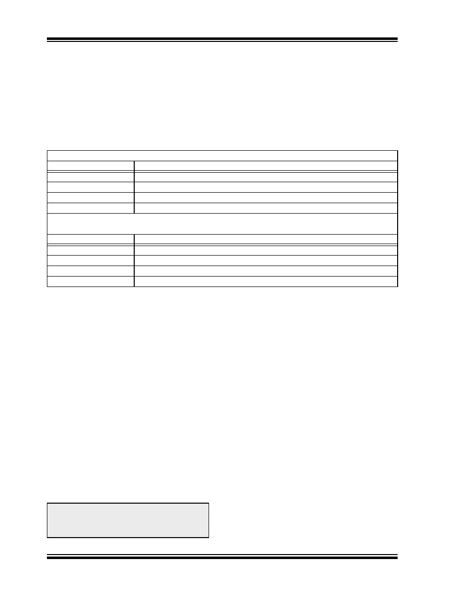
EXAMPLE 4-2:
TWO-WORD INSTRUCTIONS
4.8
Lookup Tables
Lookup tables are implemented two ways. These are:
Computed GOTO
Table Reads
4.8.1
COMPUTED GOTO
A computed GOTO is accomplished by adding an offset
to the program counter (ADDWF PCL).
A lookup table can be formed with an ADDWF PCL
instruction and a group of RETLW 0xnn instructions.
WREG is loaded with an offset into the table before
executing a call to that table. The first instruction of the
called routine is the ADDWF PCL instruction. The next
instruction executed will be one of the RETLW 0xnn
instructions, that returns the value 0xnn to the calling
function.
The offset value (value in WREG) specifies the number
of bytes that the program counter should advance.
In this method, only one data byte may be stored in
each instruction location and room on the return
address stack is required.
4.8.2
TABLE READS/TABLE WRITES
A better method of storing data in program memory
allows 2 bytes of data to be stored in each instruction
location.
Lookup table data may be stored 2 bytes per program
word by using table reads and writes. The table pointer
(TBLPTR) specifies the byte address and the table
latch (TABLAT) contains the data that is read from, or
written to program memory. Data is transferred to/from
program memory, one byte at a time.
A description of the Table Read/Table Write operation
is shown in Section 5.1.
CASE 1:
Object Code
Source Code
0110 0110 0000 0000
TSTFSZ
REG1
; is RAM location 0?
1100 0001 0010 0011
MOVFF
REG1, REG2
; No, execute 2-word instruction
1111 0100 0101 0110
; 2nd operand holds address of REG2
0010 0100 0000 0000
ADDWF
REG3
; continue code
CASE 2:
Object Code
Source Code
0110 0110 0000 0000
TSTFSZ
REG1
; is RAM location 0?
1100 0001 0010 0011
MOVFF
REG1, REG2
; Yes
1111 0100 0101 0110
; 2nd operand becomes NOP
0010 0100 0000 0000
ADDWF
REG3
; continue code
Note:
The ADDWF
PCL
instruction does not
update PCLATH and PCLATU. A read
operation on PCL must be performed to
update PCLATH and PCLATU.
发布紧急采购,3分钟左右您将得到回复。
相关PDF资料
PIC18LF8680T-I/PT
IC PIC MCU FLASH 32KX16 80TQFP
PIC16F1936-I/SO
IC PIC MCU FLASH 512KX14 28-SOIC
PIC18F24K20-I/SO
IC PIC MCU FLASH 8KX16 28SOIC
PIC18LF8585T-I/PT
IC PIC MCU FLASH 24KX16 80TQFP
XF2J-3024-11
CONN FPC 30POS 0.5MM SMT
PIC18LF6525T-I/PT
IC PIC MCU FLASH 24KX16 64TQFP
PIC18LF8621T-I/PT
IC PIC MCU FLASH 32KX16 80TQFP
PIC18F8620T-E/PT
IC PIC MCU FLASH 32KX16 80TQFP
相关代理商/技术参数
PIC18F4539T-E/PT
功能描述:8位微控制器 -MCU 24KB 1408 RAM 32 I/O RoHS:否 制造商:Silicon Labs 核心:8051 处理器系列:C8051F39x 数据总线宽度:8 bit 最大时钟频率:50 MHz 程序存储器大小:16 KB 数据 RAM 大小:1 KB 片上 ADC:Yes 工作电源电压:1.8 V to 3.6 V 工作温度范围:- 40 C to + 105 C 封装 / 箱体:QFN-20 安装风格:SMD/SMT
PIC18F4539T-I/ML
功能描述:8位微控制器 -MCU 24KB 1408 RAM 32 I/O RoHS:否 制造商:Silicon Labs 核心:8051 处理器系列:C8051F39x 数据总线宽度:8 bit 最大时钟频率:50 MHz 程序存储器大小:16 KB 数据 RAM 大小:1 KB 片上 ADC:Yes 工作电源电压:1.8 V to 3.6 V 工作温度范围:- 40 C to + 105 C 封装 / 箱体:QFN-20 安装风格:SMD/SMT
PIC18F4539T-I/PT
功能描述:8位微控制器 -MCU 24KB 1408 RAM 32 I/O RoHS:否 制造商:Silicon Labs 核心:8051 处理器系列:C8051F39x 数据总线宽度:8 bit 最大时钟频率:50 MHz 程序存储器大小:16 KB 数据 RAM 大小:1 KB 片上 ADC:Yes 工作电源电压:1.8 V to 3.6 V 工作温度范围:- 40 C to + 105 C 封装 / 箱体:QFN-20 安装风格:SMD/SMT
PIC18F4550EPT
制造商:Microchip Technology Inc 功能描述:
PIC18F4550-I/ML
功能描述:8位微控制器 -MCU 32kBF 2048RM FSUSB2 RoHS:否 制造商:Silicon Labs 核心:8051 处理器系列:C8051F39x 数据总线宽度:8 bit 最大时钟频率:50 MHz 程序存储器大小:16 KB 数据 RAM 大小:1 KB 片上 ADC:Yes 工作电源电压:1.8 V to 3.6 V 工作温度范围:- 40 C to + 105 C 封装 / 箱体:QFN-20 安装风格:SMD/SMT
PIC18F4550-I/P
功能描述:8位微控制器 -MCU 32kBF 2048RM FSUSB2 RoHS:否 制造商:Silicon Labs 核心:8051 处理器系列:C8051F39x 数据总线宽度:8 bit 最大时钟频率:50 MHz 程序存储器大小:16 KB 数据 RAM 大小:1 KB 片上 ADC:Yes 工作电源电压:1.8 V to 3.6 V 工作温度范围:- 40 C to + 105 C 封装 / 箱体:QFN-20 安装风格:SMD/SMT
PIC18F4550-I/PT
功能描述:8位微控制器 -MCU 32kBF 2048RM FSUSB2 RoHS:否 制造商:Silicon Labs 核心:8051 处理器系列:C8051F39x 数据总线宽度:8 bit 最大时钟频率:50 MHz 程序存储器大小:16 KB 数据 RAM 大小:1 KB 片上 ADC:Yes 工作电源电压:1.8 V to 3.6 V 工作温度范围:- 40 C to + 105 C 封装 / 箱体:QFN-20 安装风格:SMD/SMT
PIC18F4550T-I/ML
功能描述:8位微控制器 -MCU 32kBF 2048RM FSUSB2 RoHS:否 制造商:Silicon Labs 核心:8051 处理器系列:C8051F39x 数据总线宽度:8 bit 最大时钟频率:50 MHz 程序存储器大小:16 KB 数据 RAM 大小:1 KB 片上 ADC:Yes 工作电源电压:1.8 V to 3.6 V 工作温度范围:- 40 C to + 105 C 封装 / 箱体:QFN-20 安装风格:SMD/SMT